Quantcast
Channel: hardware accelerator – Tech Design Forum

Achronix moves into embedded FPGA

0
0

Achronix has decided to offer the FPGA technology it has developed for its own standalone parts as a set of embeddable cores in the belief that changes in the market make the concept of inserting FPGA macros into SoCs is now viable.

Steve Mensor, vice president of marketing for Achronix, said the company sees three main targets for embeddable FPGA cores: compute-server acceleration; software-defined networking equipment; and 5G wireless infrastructure. In the immediate future, the business is “going to be mostly shared between computer and wireless,” he added.

Although embedded FPGA IP has been used in commercial SoCs only rarely up to now, Mensor said the demand for lower latency between processing blocks in a system and concerns over power consumption as well as system cost make the idea of embedded FPGA cores more attractive in these systems compared. A further change in the conditions for an approach to design that has struggled in more than 15 years since the embedded-FPGA concept first appeared is one of available density in advanced processes.

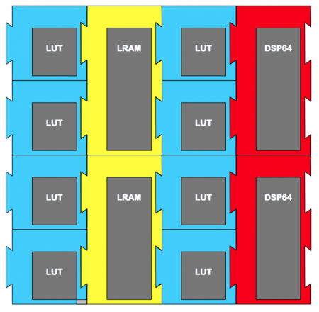
The Speedcore IP is supplied as collections of LUTs, memories and DSP elements

Image The Speedcore IP is supplied as collections of LUTs, memories and DSP elements

“You need a minimum of 50,000 lookup tables,” Mensor argued. He pointed to the available capacity on 16nm finFET-plus at TSMC, one of the IP’s target processes along with Intel’s, where Achronix’s standalone FPGAs are made. “People ask it we will port back to a process like 65nm. But there is not enough room to do anything meaningful on a process like that.”

Mentor claimed the company already has customers in place for the embedded FPGA cores – expecting to close $12m in revenue for them by the end of this year. “We have customers using 150,000 lookup tables. The can invest because of the value proposition they are getting.”

According to Mensor, the key to opening up a market for embedded FPGA lies in the desire to reduce the number of internal I/O lines in basestations and server blades, many of which today couple a custom SoC with an FPGA to cater for late design or in-system alterations to the hardware.

“None of the deals are closing because of cost or power. They are closing because of lower latency in these accelerator applications,” Mensor said, adding that the company is not shifting to an IP model. “We are not getting out of [discrete] FPGAs. A new generation of the Speedster is targeted for the end of next year.”

The FPGA IP is delivered as a hard macro compiled from a number of tiles. Some of those tiles can be DSP and memory-intensive or simply provide an array of programmable lookup tables. To try to simplify design, the tiles are linked through switch matrices that support a standard collection of interconnect bundles, from single wires up to octals. “All they have to do is be connected together by abutment,” Mensor said, adding that the macros would be supplied to fit the power grid used by the customer.

Steve Dodsworth, vice president of worldwide sales, said competition for embedded FPGA could come from 2.5D integration but noted equipment makers working on the 5G ramp-up seem to favour monolithic integration.

“We are doing a lot of research on 2.5D. It is definitely very important. I think the 2.5D market will emerge but the packaging technology is not quite there where it can become broad-based. The problem is if you talk about organic substrates, you are about having to use short-reach series,” said Dodsworth.

The need to deploy serdes interfaces on the dice sitting on an organic substrate means users cannot take advantage of the denser, lower-power interconnect that can be used between cores sitting on a monolithic IC.

“With silicon, you are facing yield issues,” Dodsworth added. “And you are limited in terms of substrate size to [the reticle limit of] 26mm x 34mm.

“With 2.5D, the cost point isn’t there. In wireless infrastructure, they ship a million-plus ASICs,” Dodsworth claimed, which puts the onus on monolithic integration. “But as mask costs are very high on the processes they need to use, they have to squeeze as much flexibility out of every mask start they do. Putting FPGA on the die gives them the flexibility they need because the [5G] standards aren’t there yet.”
ARM brings security to Cortex-M family

0
0

ARM has launched the first of a series of Cortex-M series microcontrollers based on the V8M architecture that incorporate the Trustzone security mechanism.

“The principle of Trustzone is to isolate resources that need to kept secure from non-trusted software or hardware,” said Ian Smythe, director of marketing programs in ARM’s CPU group, noting that the design of the Cortex-M23 and M33 and the support infrastructure the company has developed extends the protection “to all the IP that connects the system together and not just the CPU alone”.

Smythe added: “The two processors have been designed together to make sure it is as easy as possible to move from one to the other.”

Cortex-M successors

Nandan Nayampally, vice president of marketing in ARM’s CPU group, said: “The Cortex-M33 succeeds the Cortex-M3/M4 line while the Cortex-M23 takes on some of the very constrained applications that the Cortex-M0 and M0+ championed. The M33 is configurable for DSP and floating-point processing.”

According to Smythe, the M33 offers 20 per cent higher performance per clock cycle than the M4.

To provide a secure infrastructure for trusted software running in the core to talk securely to onchip peripherals, ARM has introduced AHB5. The interconnect add security-control bits to the address lines to prevent unwanted access to sensitive peripherals. To support the incorporation of a hardware root of trust, ARM has designed a cryptocontroller core that interfaces to the central processor through the AHB5 interconnect. In addition, ARM has developed a tightly coupled coprocessor interface for custom accelerators.

“If you take a smart sensor, it may use special processing such as Kalman filtering and then compress the data to send it over a wireless link,” said Smyth. Using the coprocessor interface allows special-purpose hardware to be added to the core “without fragmenting the ecosystem”.

Coprocessor interface

Thomas Ensergueix, director of product marketing at ARM, said: “The coprocessor interface acts as a high-efficiency bus that goes directly to the processor and allows you to exchange data between the processor and coprocessor. The bus can transfer two registers at the same time – it passes data and instructions back and forth with high efficiency.”

To maintain security, the coprocessor does not have access to the main memory bus. All data passes through the processor. Ensergueix pointed out that the coprocessor can operate in both secure and non-secure modes depending on the state of the host processor at the time.

Nayampally said that, on a 40nm process, a full implementation of the Cortex-M33 should take up around 0.1 square millimetres of die area. “40nm is coming into its own as a process technology for IoT,” he added. By comparison, the Cortex-M4 consumes 0.04 square millimetres on a typical 40nm process.

So far, nine companies have licensed one or both of the microcontroller cores, Nayampally added.

Cloud service

As well as introducing the new processor cores, ARM launched a cloud-based device-management and configuration service. Michael Horne, vice president of sales for ARM’s IoT group, said: “Conversations with customers indicate device management is becoming a limiting factor on their ability to deploy IoT.”

Horne said the mBed Cloud service will support any cloud software used by the customer, using standard CoAP and LWM2M protocols to communicate with managed devices, which can run either mBed OS natively or for a subset of the services, a client application ported to Linux or a third-party RTOS running on an ARM or other processor architecture. He added: “mBed OS has the ability to natively talk to the mBed Cloud.

“In terms of business model, it is delivered as a service from the cloud. It is structured like the business model of most Saas companies,” Horne said.

MTAPI library adds patterns for heterogeneous multicore

0
0

Siemens has published version 1.0 of its task-management library Embedded Multicore Building Blocks (EMB2) to Github. The latest major release of the open-source library introduces C++ wrappers, plugins for GPU programming, and a variety of design patterns to speed up the development of heterogeneous multicore applications for embedded systems.

Initially released in autumn 2014 in its version 0.2 form following internal development by the Siemens Corporate Technology team, EMB2 uses the Multicore Task Management Application Programming Interface (MTAPI) developed by the Multicore Association as a standarized way to divide tasks across different types of processor in manycore systems and coordinate them.

Tobias Schüle, project manager at Siemens Corporate Technology, said one of the motivations for basing EMB2 on MTAPI was to overcome the problem of porting applications from one manycore platform to another even with different memory hierarchies.

“MTAPI was designed with heterogeneous embedded systems in mind,” Schüle said. “It does not just use shared memory and compute nodes can have different instruction-set architectures. All the passing of parameters and getting results from tasks is completely hidden in the library. It greatly simplifies the programming of such systems from a developer’s perspective.”

Design patterns

MTAPI’s approach splits workloads into groups: tasks and queues. “Queues were a requirement for telecom network routers and so on, where you have streams of data to process in a certain order.”

To further help with application-specific requirements, the EMB2 developers created a set of design patterns to reflect common multiprocessing situations “and release developers from the burden of thread management synchronization and so on”, Schüle said.

The team placed a strong emphasis on lock-free synchronization schemes to improve overall performance. “We don’t want to use blocking synchronization structures like mutexes,” Schüle said. “We also wanted resource awareness and determinism. For safety-critical systems you are able to avoid the use of dynamic memory allocation.”

The EMB2 library supports the ability to dynamically schedule and allocate tasks to different processes. “Each job has actions such as an FFT. That FFT could be implemented on GPU, hardware, FPGA or just a CPU. As an application developer you don’t have to care about where the task is executed. You can leave the decision up to the scheduler,” Schüle claimed, noting that the application will need variants compiled of the FFT task that are suitable for each of the compute resources that can be used. But with the binaries available, “you can do load balancing dynamically”.

EMB2 has a default scheduler based on resource availability that can be swapped for a different scheme, such as one that takes into account power-management considerations. “We have a plug-in architecture so you can write your own to support special hardware such as custom processors in FPGAs,” he added. The group has added readymade plugins for environments such as CUDA for GPU programming.

Schüle said the C++ wrappers in the latest release make it easier to use the C-based MTAPI API in the object-oriented language.

Group to build CCIX accelerator test chip

0
0

ARM, Xilinx, Cadence Design Systems, and TSMC have agreed to produce a test chip for the Cache Coherent Interconnect for Accelerators (CCIX) project. The test chip is designed to demonstrate how many-core ARM processors can work with programmable-logic accelerators in high-performance servers.

The test chip will be built on TSMC’s 7nm FinFET process node and will include a number of ARM DynamIQ processor cores sharing access to memory and peripherals using the CMN-600 coherent on-chip bus. Cadence is provide I/O, memory, and PCIExpress IP plus as well as the CCIX interface, which will connect to Xilinx Virtex FPGAs.

Babu Mandava, senior vice president and general manager of Cadence’s system-IP group, said: “The CCIX industry standard will help drive the next generation of interconnect that provides the high-performance cache coherency that the market is demanding.”

“Artificial intelligence and deep learning will significantly impact industries including media, consumer electronics and healthcare,” said Cliff Hou, TSMC vice president for R&D and technology platforms.

Noel Hurley, vice president and general manager for ARM’s infrastructure group, said: “The test chip will not only demonstrate how the latest ARM technology with coherent multichip accelerators can scale across the data centre, but reinforces our commitment to solving the challenge of accessing data quickly and easily. This innovative and collaborative approach to coherent memory is a significant step forward in delivering high-performance, efficient data centre platforms.”

The CCIX project is one of three separate initiatives aimed at providing high-speed interfaces between manycore SoCs and accelerators. Gen-Z focuses on memory-centric architectures and OpenCAPI was derived from IBM’s work on accelerators for the Power architecture.

Cloud makes hardware acceleration more accessible

0
0

At this year’s Design Automation Conference (DAC), Cadence Design Systems and Mentor, a Siemens business, publicly announced they had put hardware emulators in the cloud to make it easier for customers to access accelerated verification. The moves may help promote the use of other forms of hardware acceleration dedicated to EDA tasks.

During a session at the conference to describe to users how its cloud service operates, Jean-Marie Brunet, marketing director of Mentor’s emulation business, said the company has done extensive planning for the service: “We worked with Amazon for over a year on this.”

Among the concerns were how long it would take to send design data to the emulator. ”If it takes a couple of days to send to the box and it take three hours to run, that’s not a good value proposition,” Brunet said, adding the ability to compile the RTL for emulation close to the emulator itself is important.

First experiments

Rajesh Shah, CEO of IP designer Softnautics, said the company was keen to experiment with cloud-based emulation and seized on the opportunity to test Mentor’s offering. “We would like to have design in the cloud and enable customers to build systems or subsystems in the the cloud.”

Shah said experiments that involved stimuli from a C testbench demonstrated that the data transfers could take place quickly, with about 3Gbyte of results and other data transferred back in about five minutes.

Brunet said: “It took us a while to put this together but it’s in place. It’s the same flow you are running today. Except you have no idea where the box is.”

In practice, there will be some effect from geographical location. Response times, Brunet said, “will be related to the amount of hardware in a geographical region. Go across a region you may have some degradation in latency”.

Although one of the applications of cloud-based emulation is to absorb peak demand towards the end of a project, the capacity available online will limit how much peak demand the service can absorb. Brunet said, at least in the early days of the service, Mentor would look to establish a more consistent baseline usage with customers and “enable peak usage once a baseline has been established”.

Security assurances

The rollout of services like emulation in the cloud are beginning to demonstrate that EDA users are becoming more comfortable with the idea of sending design data to third-party server farms. Mentor worked with Amazon Web Services (AWS) to try to demonstrate that data would be protected.

“We had a lot of questions from the field: is this secure? When you see Department of Defense and national security certificates: you can say ‘that is OK’,” Brunet claimed. “It’s very secure.”

David Pellerin, head of worldwide business development for high-performance computing at AWS, said: “You’ve got to have security. We work with third party auditors to demonstrate that. Large enterprises now understand that they can operate in a more secure manner than with legacy infrastructure.”

Although, Pellerin acknowledged the concerns over security, he said: “We’ve gone past that now.” What is happening now is that EDA users are beginning to see the end of the road for much of their internal infrastructure.”

Pellerin added: “The pattern we have seen in EDA is to similar to other computer-aided engineering areas. You have a dedicated data center with various servers of different vintages. It’s not really flexible. You can’t have different resources available during short bursts. The difference when we move to cloud is you can create that same environment but it’s now flexible and scalable. I can scale up and I can scale down. We have been seeing tremendous productivity in areas such as drug discovery and proteomics. And now in EDA.”

In an interview with TDF at DAC, Metrics Technologies president and CEO Doug Letcher, said he perceives the same shift in attitude among users to putting more design data into the cloud. “What we’re seeing is that, often, engineers in the field have this opinion ‘this is awesome but management won’t let me do it’. But the management people now see it as being strategic to IT.

“Companies have mandates to not build data centres on their own,” Letcher added. “Engineers in the field haven’t caught up with the change in attitude in management. One vice president at a relatively large semiconductor company said ‘we’ve moved our financial, customer support and legal data into the cloud. Am I really that worried about the RTL?”

Acceleration options

Having started with a software-based simulator that runs on cloud servers, Metrics is now beginning to look at offering hardware-based acceleration. Shortly before the conference, the company announced its intention to merge with Montana Systems, which is developing a simulation accelerator for SystemVerilog workloads. Letcher said he sees a major advantage to putting acceleration into the cloud as a service instead of selling the necessary hardware to customers. They will be able to access the accelerator by selecting a different option and then running the testbench as normal.

“Emulation takes some time to port. Our target is maybe five to twenty times faster than software-based simulation but it’s zero effort,” Letcher said. “And it takes away the idea that I have to buy a box upfront. Over the course of next year we will be putting that product together.”

At the other end of the convenience scale for logic verification is the deployment of field-programmable gate arrays (FPGAs) into the cloud through services such as F1 from AWS. In his keynote at DAC, UC Berkeley Professor David Patterson said he saw the availability of these cloud-based FPGAs as being part of a rapid prototyping flow for a new wave of designs. Though they have to be specifically compiled for an FPGA platform, as with existing virtual-prototyping boxes, the ability to rent the hardware for short periods of time could be instrumental in moving to more agile design techniques.

“It takes months for chips to come back from the fab. So how do you do iteration? You can use simulation at the C++ level but those are still pretty slow,” Patterson said. “The next step is FPGAs. For some people they don’t want the hassle of buying FPGAs and setting up a lab. But you don’t have to do that: FPGAs are in the cloud. You can rent cloud service. It’s a remarkable opportunity.”

Netronome launches chiplet initiative for network-accelerator SIPs

0
0

Data-center networking specialist Netronome has recruited a number of silicon makers and IP suppliers to a standard for chiplet designs that can be used in SIPs for edge computers and servers.

Netronome has said it is collaborating with six companies so far: Achronix, GlobalFoundries, Kandou, NXP, Sarcina, and SiFive. They aim to develop an architecture and a set of interface and design specifications for chiplets to make it easier for SIP integrators to mix and match processors, accelerators, memory, and I/O controllers and avoid the need to port all of them to the same semiconductor process.

The Open Domain-Specific Accelerator (OSDA) is intended to cover standards for implementing SIP flows based on known-good die as well as the interconnect networks the chiplets will use to communicate and the software stack they run on top. The hope is this will lower the hardware and software costs of developing and deploying domain-specific accelerators. In principle, any vendor’s silicon die can become a building block that can be used in a chiplet-based design.

“The end of Moore’s Law will increase the use of domain-specific accelerators to meet power-performance requirements in cloud infrastructure, network infrastructure and IoT/wireless edge applications,” said Bob Wheeler, principal analyst at The Linley Group. “With its modular approach, the open domain-specific accelerator architecture could change the chiplet paradigm from single-vendor solutions to a world of choice, thereby enabling OEMs and operators to develop and deploy advanced SoC solutions.”

“The use of AI and the need for power-efficient, high-throughput parallelism is driving the growth of accelerators. However, the high cost and complexity of accelerator development is a major factor restraining growth,” said Steve Mensor, vice president of marketing at Achronix. “We are delighted to join and bring our embedded FPGA technology to the ODSA Workgroup to enable customers to bring open, cost-efficient accelerator products to market.”

Amin Shokrollahi, founder and CEO at Kandou, said the company sees its serdes technology as being important for chiplets that communicate inside a multichip module. Sam Fuller, director of marketing at NXP said the company aims to provide multicore Arm SoCs to companies building devices based on the chiplet standard.

Netronome said the ODSA is just starting work and is open for contributions as well as accepting new members of the workgroup. Companies and industry partners wishing to learn more and participate can contact: odsa@netronome.com.

PCI may provide key to OCP chiplet standard

0
0

A group set up by Netronome and a small group of IP and silicon vendors to create standards for chiplets to be used in server accelerators is looking to base the core inter-die communications interface on the PIPE protocol of PCI. The approach could avoid the need to pick one of many emerging low-power physical-layer interfaces.

Late last year, Netronome recruited GlobalFoundries – which has decided to focus on multichip integration since giving up 7nm development – along with Achronix, NXP, SiFive and others to form the Open Domain-Specific Architecture (ODSA) Workgroup. This effort has now been absorbed into the Open Compute Project (OCP) organization formed to create standards for data-center products.

During a talk on ODSA at last week’s OCP Summit (March 15, 2019), Netronome engineer Bapi Vinnakota said the number of companies involved with ODSA has grown to 35 and that the workgroup plans to build a proof-of-concept multichip module suitable for use on an OCP-compatible daughtercard that will likely include external photonics ports using existing parts provided by members, including Achronix, Avera Semiconductors, Netronome, Sarcina and zGlue. The exercise will help identify issues with integrating chiplets from multiple vendors. In tandem, the group wants to define an “open cross-chiplet fabric interface”, he noted.

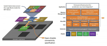
The OSDA Workgroup wants to focus chiplet interconnect standard on the PCI PIPE abstraction

Image The OSDA Workgroup wants to focus chiplet interconnect standard on the PCI PIPE abstraction

Vinnakota said, with the exception of system-in-package (SIP) products that use HBM for high-speed memory integration, most chiplet-based designs use devices designed by a single vendor. Examples in use today include the larger FPGAs made by Intel Programmable Systems Group (PSG) and Xilinx. In 2015, Marvell said its AP806 and Armada A3700 products were based on chiplets integrated into what the company called ”virtual SoCs” based on an inter-die extension of its onchip bus interface called MoChi. The physical-layer interface in the chiplets uses IP from one of the ODSA Workgroup’s first members: Kandou.

The motivation for the work is to reduce the cost of designing accelerators for server applications that, because of their domain-specific nature will serve markets too small to justify the cost of designing complete SoCs on leading-edge processes. “Only the biggest can afford to build these devices,” Vinnakota said.

A second problem Vinnakota argued is that, for those startups and internal groups trying to create accelerators, much of their time is spent building the ancillary functions that will hook their IP into the server infrastructure. He cited one startup he had talked to which had raised Series B funding but found two-thirds of that would be needed to design and build the management processors and I/O needed to realize a complete accelerator SoC.

By moving development to a chiplet-based design, he argued much of the funding could be focused on core competencies: “Don’t burn your dollars in building this large monolithic die. All accelerators have three or four things in common but only one is specific to acceleration.”

A key development in the evolution of chiplet-based SIPs is the emergence of low-power serdes IP. A white paper produced by the group late last year identified a number of options that can offer energy consumption down to the level of a couple of picojoules per bit that is needed to make the architecture feasible.

Rather than attempt to pick one of these candidates, the Vinnakota said the current aim of the group is to work at a higher level so that users can decide on which PHYs they implement and demand from suppliers. Already supported by accelerator-focused PCB-level standards such as CCIX, the group sees PCI’s PIPE as a potential platform for the interface standards. This could support both cache-coherent interconnects such as CCIX, OpenCAPI and SiFive’s TileLink as well as non-cache-coherent bulk-transfer links.

Xilinx aims for software flow with Vitis

0
0

Xilinx has released the first version of its Vitis development environment as the company aims to capture a user base that is more used to software than hardware tools.

With customers adopting AI as part of the platform, the FPGA maker sees a blurring of the skill sets. Ramine Roane, vice president of software and AI product management, said customers such as Samsung were looking to use machine learning in applications such as 5G deployment. The favoured implementation engine for AI in the forthcoming Versal family will be a programmable processor, which demands more of a software approach although the engine might talk to hardware generated using Vivado.

“Every segment we are addressing is either looking at AI or deploying AI,” Roane said.

The tools in the initial version of Vitis target the 28, 20, and 16nm generations. “We will see general availability next year for Versal,” Roane said.

To capture users in segments such as biotech, financial technology and ADAS R&D, Xilinx has take the approach that is broadly similar to that used by DSP vendors: offering libraries of parallelised functions called by a program. Runtime components, which are provided in open-source form, manage the transfer of data between the modules and I/O ports.

“Our goal is to get similar performance [to HDL]. That's why we are using libraries,” Roane said.

In Vitis, developers have access to high-level synthesis from C through the use of pragmas to define how user functions are parallelised. However, the tools are intended to be able to do loop unrolling and similar tasks automatically based on available resources.

Rob Armstrong, director of technical marketing for AI and software acceleration at Xilinx, said one issue with developing for programmable hardware remains compile time. To address this, Vitis offers an emulation environment designed to show bottlenecks and other potential problems before the engineer commits to to a hardware compile. It represents the application in terms of a data flow graph.

“We are appealing to a new market of developers who don't have a hardware background or RTL skills. We are trying to present data to them that isn't overwhelming,” Armstrong said. At the same time, he added: “The developers we are targeting are not unsophisticated. Engineers who use GPUs for acceleration understand things like cache behavior. They aren't the JavaScript guys.”


DAC prepares for winter show

0
0

The program for the Design Automation Conference, which returns to a physical format in December, is online and is running its I Love DAC promotion for free access until the end of this month (October 31st, 2021).

DAC returns for its 58th year, again combining the technical program with a line up of Keynotes and SKYTalks. This year DAC will use a hybrid format for both in-person and virtual attendance. In addition, for the first time, DAC attendees will also have access to attend both the SEMICON West expo being held at Moscone South and the RISC-V Summit exhibits at Moscone West.

AI forms the basis of a number of the keynotes and SKYtalks this year. Jeff Dean senior vice president of Google Research and Google Health will kick off the keynotes by looking at the potential of machine learning learning for hardware design, following the publication of some of the company’s work in this area in the early summer.

Bill Dally, chief scientist at nVidia, will look at the role of GPUs in machine learning both for driving end-user applications and in the EDA flow. His talk aims to cover near-term uses for GPUs and a longer-term view of what is possible.

As machine learning takes hold in areas such as EDA, the question becomes whether the process will be a competition of humans vs machine or something far less contentious. Duke University professor of computer engineering Mary Cummings will focus on how to allocate roles and functions to humans and computers as the computers continue to improve in their understanding of EDA and other tasks.

AI will also feature strongly in the SKYtalks with presentations from William Chappell, CTO of Azure Global and IBM fellow Kailash Gopalakrishnan. Sam Naffziger, AMD senior vice president, will tackle the subject of cross-disciplinary innovations required for the future of computing.

For this year’s program the technical program committee has selected 215 papers from a total of 914 submitted manuscripts. In addition, 199 industry focused submissions were reviewed with 70 accepted for presentation.

Registration for the I Love DAC free three-day pass sponsored by Cliosoft, Empyrean and Menta is open through October 31, 2021.

The 59th DAC return to the summer next year and will be held at Moscone West Center in San Francisco, CA, from July 11–15, 2022. DAC will co-locate with SEMICON West 2022 which will be held July 12–15 at Moscone North and South Halls.

Open-source EDA grapples with the incentives issue

0
0

This summer, the project and funding that led to the creation of the OpenRoad open-source RTL-to-GDS toolchain draws to a close. In 2018, US defense research agency DARPA backed the development of the tools as part of the IDEA program managed off by ZeroASIC founder Andreas Oloffson during his time at the organization.

Over the four years, OpenRoad has gained traction in some communities, along with a variety of other open-source projects, such as Verilator, which has received renewed attention from RISC-V work. A key target of IDEA and the IP-focused POSH was military R&D and the DEVCOM Army Research Laboratory has employed OpenRoad in some of its projects.

More widely, there are lingering concerns about the compatibility of open-source and commercial legal agreement. Some such as the MIT license are easy to deal with

“I’ve never seen a contract that’s so short,” said Oloffson during a conference panel on open-source EDA at DAC in San Francisco last week.

License details

Others raise issues of ‘infection’ where it becomes impossible to use both commercial and open-source components without using one in some instances breaching the terms of the other. A key issue is what IP needs to be released to the community once an open-source component has been integrated, although this may be a larger problem in open-source hardware rather than EDA tools. Proponents point to the growing acceptance of open source within the software domain and the eager participation of companies who once favoured purely proprietary offerings. Without this widespread backing, the data-center market that is now so important to high-end chip development would probably not look nearly so lucrative to hardware designers.

Chips Alliance general manager Rob Mains noted in a DAC Pavilion panel: “You have to be very careful to pay attention to the license agreements, which is not something the average engineer pays attention to.”

However, for Peter Gadfort’s small team at DEVCOM Army Research Laboratory, OpenRoad’s licensing is considerably easier to deal with than those for proprietary tools. “We are just three people working on energy-efficient, trusted, reconfigurable computing. We also get to act as mini-lawyers, which can be painful,” he explained.

A major issue is the now common use of time-limited licensing. “That can leave us without tools for a long time. And it is often difficult to get licence periods to match project time.

“Open source helps us do research to help the customer: the Department of Defense. Using more of the outcomes from IDEA and POSH like OpenRoad lets us iterate faster. We are currently working on taping out to Intel 16 using OpenRoad. The level of integration we are aiming at is just not practical in a closed-source environment. And we dont have to worry about licence issues,” said Gadfort.

It was not entirely smooth-sailing, Gadfort added. “When we started using open-source tools, the documentation was a challenge. But we were able to give feedback and make things more user friendly. Coexistence with commercial tools is truly viable, which is important as a lot of EDA flows pingpong in and out of tools.”

Mix and match

Though they won’t replace all tools in a flow, at least not in the foreseeable future, commercial chip-design teams see clear benefits in the open-source approach around collaboration. Mamta Bansal, senior director of engineering at Qualcomm, said: “Open source has the potential to lower the barrier to contribute, customise and differentiate. Can draw parallels with other open source. Very possible for all of us to contribute to the EDA community.”

Noel Menezes, director of strategic CAD at Intel Labs, questioned whether the incentives are in place to make open-source EDA viable long-term. “There has to be a virtuous cycle that establishes itself.”

Open-source EDA tools are far from new though as SPICE was developed before the copyleft licensing associated with free and open-source software (FOSS) it lacks the association. The prior heyday of such open-source software was in the 1980s, Menezes said. “But the incentives went away.”

“Now, post-IDEA, it’s better again. OpenRoad has been very successful. But my fear is that if you don’t have incentives to continue open sourcing now it’s reaching the end of its four-year program, that will be a problem,” Menezes added.

Oloffson said people working on open-source projects need to “check in for the long road. There is a lifetime of open-source maintenance to be done: Verilator is now over 20 years old.”

Chuck Alpert, senior software group director at Cadence Design Systems, said: “At the end of the day, academic culture just isn’t suited for this.”

Alpert explained the pressure to publish novel experiments does not mix well with the need to continue long-term, incremental work on software. On top of that, he noted, “academic-tenure culture doesn’t really foster a team spirit. I think that’s a big challenge”.

Training advantage

At the same time, open-source will be invaluable to the academic pipeline into industry, Alpert said: “This has to happen. The biggest value of open source is talent creation. The people who aren’t just going to run to the Facebooks and Googles: OpenRoad is training them. We want those people. We need people trained in EDA and living it so they ultimately can become our future leaders.”

Commercial interest will be vital if long-term academic support is hard to envisage. Gadfort said the open-source ecosystem needs sustainable business models. “If they are to succeed, companies need a viable path to generate income as well as foundry support.”

Menezes argued open-source projects need not try to do everything in the flow and would probably be more successful by not attempting to compete head-on. He said he favors the relatively new area of domain-specific languages (DSLs). “You have to come up with some disruptive complementary ideas. DSL may be the right disruptor for open-source EDA. [The EDA industry] continues to solve some big problems. I would not recommend open-source to go there.”

One reason for seeing DSL as a potential winner for open source is that it is an area that provides a way to optimize the code and architecture of accelerators, which are increasingly becoming the engines of high-performance computing. The wide variety of architectures and software inputs provides good reasons for seeing ecosystems build around open-source tools that bring the software and hardware elements together and allow co-operative experimentation. Bansal said the ability, in general, to go into the tools to try different things will be invaluable. “We need a playground. We don’t have that today. Open source gives you that playground if structured the right way.”


Latest Images